NXP Semiconductors
BAS21AVD
High-voltage switching diodes
BAS21AVD
All information provided in this document is subject to legal disclaimers.
? NXP N.V. 2013. All rights reserved
Product data sheet
1 August 2013
3
/
11
Symbol
Parameter
Conditions
Min
Max
Unit
Per device; one diode loaded
[1]
-
250
mW
Ptot
total power dissipation
Tamb
≤ 25 °C
[2]
-
295
mW
Tstg
storage temperature
-65
150
°C
Tj
junction temperature
-
150
°C
Tamb
ambient temperature
-65
150
°C
[1]
Device mounted on an FR4 Printed-Circuit Board (PCB), single-sided copper, tin-plated and standard
footprint.
[2]
Device mounted on an FR4 PCB, single-sided copper, tin-plated, mounting pad for cathode 1 cm2.
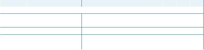
9.
Thermal characteristics
Table 6.
Thermal characteristics
Symbol
Parameter
Conditions
Min
Typ
Max
Unit
Per device; one diode loaded
[1]
-
-
500
K/W
Rth(j-a)
thermal resistance
from junction to
ambient
in free air
[2]
-
-
425
K/W
Rth(j-sp)
thermal resistance
from junction to solder
point
[3]
-
-
140
K/W
[1]
Device mounted on an FR4 PCB, single-sided copper, tin-plated and standard footprint.
[2]
Device mounted on an FR4 PCB, single-sided copper, tin-plated, mounting pad for cathode 1 cm2.
[3]
Soldering point of cathode tab.
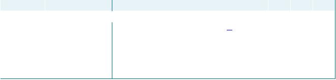
10.
Characteristics
Table 7.
Characteristics
Symbol
Parameter
Conditions
Min
Typ
Max
Unit
Per diode
IF
= 100 mA; T
amb
= 25 °C
-
-
1
V
VF
forward voltage
IF
= 200 mA; T
amb
= 25 °C
-
-
1.25
V
VR
= 200 V; pulsed; t
p
≤ 300 μs;
δ
≤ 0.02 ; T
amb
= 25 °C
-
25
100
nA
IR
reverse current
VR
= 200 V; T
j
= 150 °C
-
-
100
μA
Cd
diode capacitance
f
= 1 MHz; V
R
= 0 V; T
amb
= 25 °C
-
0.6
5
pF
trr
reverse recovery time
IF
= 30 mA; I
R
= 30 mA; T
amb
= 25 °C;
RL
= 100 Ω; I
R(meas)
= 3 mA
-
16
50
ns


发布紧急采购,3分钟左右您将得到回复。
相关PDF资料
BAS21DW-7
DIODE ARRAY 200V 200MA SC70-6
BAS21SLT1G
DIODE SWITCH DUAL 250V SOT23
BAS21TM-7
DIODE ARRAY 250V 250MA SOT26
BAS21TW-7
DIODE ARRAY 250V 200MA SOT363
BAS28,215
DIODE SW 75V 215MA HS SOT143B
BAS31
DIODE SS 120V 200MA SOT23
BAS35
DIODE GEN PURP 120V 200MA SOT-23
BAS40-04LT1G
DIODE SCHOTTKY DUAL 40V SOT23
相关代理商/技术参数
BAS21AW
制造商:NXP Semiconductors 功能描述:DIODE SWITCHING 250V 0.25A SOT323 制造商:NXP Semiconductors 功能描述:DIODE, SWITCHING, 250V, 0.25A, SOT323 制造商:NXP Semiconductors 功能描述:DIODE, SWITCHING, 250V, 0.25A, SOT323; Diode Type:Switching; Diode Configuration:Dual Common Anode; Repetitive Reverse Voltage Vrrm Max:250V; Forward Current If(AV):225mA; Forward Voltage VF Max:1.25V; Operating Temperature Min:-55C;RoHS Compliant: Yes
BAS21AW,115
功能描述:二极管 - 通用,功率,开关 DIODE SW 200V 200MA HS UMT3 RoHS:否 制造商:STMicroelectronics 产品:Switching Diodes 峰值反向电压:600 V 正向连续电流:200 A 最大浪涌电流:800 A 配置: 恢复时间:2000 ns 正向电压下降:1.25 V 最大反向漏泄电流:300 uA 最大功率耗散: 工作温度范围: 安装风格:SMD/SMT 封装 / 箱体:ISOTOP 封装:Tube
BAS21AW115
制造商:NXP 功能描述: 制造商:NXP Semiconductors 功能描述:
BAS21BPT
制造商:CHENMKO 制造商全称:Chenmko Enterprise Co. Ltd. 功能描述:FAST SWITCHING DIODE VOLTAGE RANGE 250 Volts CURRENT 200 mAmpere
BAS21C
功能描述:二极管 - 通用,功率,开关 Switching diode 225 mW RoHS:否 制造商:STMicroelectronics 产品:Switching Diodes 峰值反向电压:600 V 正向连续电流:200 A 最大浪涌电流:800 A 配置: 恢复时间:2000 ns 正向电压下降:1.25 V 最大反向漏泄电流:300 uA 最大功率耗散: 工作温度范围: 安装风格:SMD/SMT 封装 / 箱体:ISOTOP 封装:Tube
BAS21C _R1 _00001
制造商:PanJit Touch Screens 功能描述:
BAS21C RF
制造商:SKMI/Taiwan 功能描述:Diode Switching 250V 0.2A 3-Pin SOT-23 T/R
BAS21C RFG
功能描述:DIODE ARRAY GP 250V 200MA SOT23 制造商:taiwan semiconductor corporation 系列:- 包装:带卷(TR) 零件状态:在售 二极管配置:1 对共阴极 二极管类型:标准 电压 - DC 反向(Vr)(最大值):250V 电流 - 平均整流(Io)(每二极管):200mA 不同 If 时的电压 - 正向(Vf:1.25V @ 200mA 速度:小信号 =< 200mA(Io),任意速度 反向恢复时间(trr):50ns 不同?Vr 时的电流 - 反向漏电流:100nA @ 200V 工作温度 - 结:-55°C ~ 150°C 安装类型:表面贴装 封装/外壳:TO-236-3,SC-59,SOT-23-3 供应商器件封装:SOT-23 标准包装:3,000